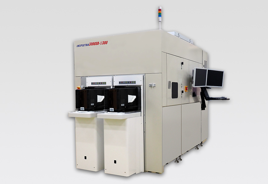
Optical Semiconductor Wafer Inspection System “INSPECTRA®”
Our INSPECTRA® is AOI Wafer Surface and Appearance Inspection System and contributes to improve customers' production efficiency and yield for many years. It can not only check crystal defects by PL (Photo Luminescence) and back side but also realize high-speed and -sensitive inspections on various kinds and shapes of wafers including compound semiconductor, for example SiC and GaN etc., at all processes regardless front- or back-end process.
INSPECTRA® can contribute to improve customers' added value of your products and is ideal for various kind of semiconductors, power semiconductors, µLED and MEMS
We are pleased to offer an on-site demonstration in Munich or sample evaluation by taking customers' sample.
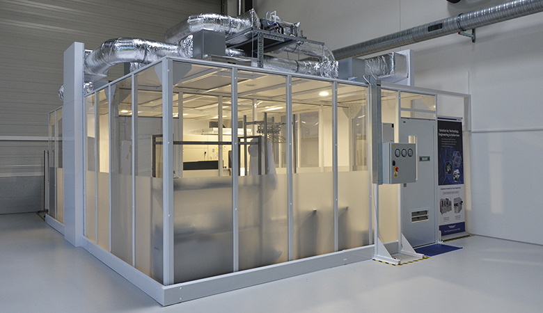
Information of Demonstration Room
Our Demonstration Room in Munich offers customers in Europe a flexible opportunity to experience INSPECTRA® fostering a deeper understanding and accelerating customers' evaluation.
Service and Demonstration office
Am Gfild6 85375 Neufahrn bei Freising Germany
Tel: +49-8165-40996-70